• ±7μm Placement
• Cpk ≥ 1.67
• 0 Defect for Automotive Application

• Vibration Suppression Technology
• Real-Time Correction Technology
• Years of Stable & Reliable HVM

• +20% High Throughput
• Enhanced Overall OEE

• MES Traceability
• Unmanned Automation Line
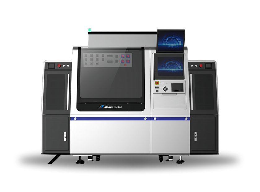
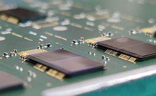
• Automotive COB Process
| Item | Specifications |
| End Market | Consumer / Automotive |
| Application | Smartphone / Automotive CMOS Modules, LiDAR Modules |
| Material Handling | 4~12" Wafer, JEDEC Tray, Waffle Pack etc. |
| Process | COB, BGA, DAF |
| Die Placement | XY: ≤±7μm@3σ; θ: ≤±0.1°@3σ |
| UPH | ≥2200 (Smartphone COB, ≥36 pcs / Strip); ≥1000 (Automotive COB, ≥18 pcs / Strip) |
| Footprint & Weight | Configuration Dependent |
Placement
Thin Die
Stacking
Class


• ±5μm Placement
• Friction-Free Precise Force Control
• Vibration Suppression
• 25μm Die Thickness
• 32-Hi
• Key OSAT / IDM Running HVM

• Leading UPH & OEE
• Compatible with All DRAM & Flash Processes
• Support DAF & Epoxy

• Patented Crack-Free Technology
• Deep Learning AOI
• Support Industry 4.0
| Item | Specifications |
| Wafer | 6"~12" |
| Die Size | 0.8~25mm |
| Die Thickness | ≥25μm |
| Bond Force | 0.5~50N (70N Optional) |
| Die Placement | ±5μm@3σ |
| Process | DAF & Epoxy |
| UPH | Material Dependent |
| Item | Specifications |
| Strip Length | 130~300mm |
| Strip Width | 55~100mm (Optional <55mm) |
| Heater Block | Max 250°C (±5°C) |
| Die Stacking | YES |
| Packages | BGA / QFP / QFN etc. |
| Footprint (mm) | 2292x1551x1900 (LxDxH) |
| Weight | 2450kg |
Placement
Industry 4.0
Multi-chip Mounting
Material Traceability; Self-Diagnosis


• XY Placement: ±3μm@3σ
• Theta Rotation: 0.07°@3σ
• Force Control: 0.1-10N±10%
• Precise BLT Control

• Industry-Leading UPH
• Extremely User-Friendly
• High Speed Mode with ±10μm Placement

• Easy Process Changing
• Easy Product Conversion
• Auto Tool Changing

• Support SECS / GEM, Inline, OHT, AGV
• Post-Disp / Bond Smart Inspection
• FM / Crack Detection
• Self-Diagnosis
| Item | Specifications |
| Application | Photonics, Transceiver, SiP, LIDAR, Camera Module, etc. |
| Die Size | 0.15-25mm |
| Die Thickness | 0.025-7.0mm |
| Bond Force | 0.1-10N±10% |
| Die Placement | ±3μm@3σ |
| Attach Process | COB, FC, DA with Epoxy / Silver Paste / UV Glue |
| Item | Specifications |
| Substrate | L: 130-260mm x W: 55-140mm |
| Material Handling | FR4, Leadframe, Strips, Carrier, Boat, Ceramics, 6"-12"Wafer, Gel-pak, Waffle Pack, Tray, Feeder |
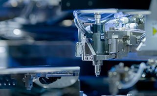
| Bondhead | 6 Collets Auto Changing, Heating, UV, Confocal Height Measurement |
| Ejector System | 5 sets Auto Changing |
| Footprint(mm) | 1240x1553x2060 (LxDxH) |
Placement
UPH
Stacking
Class


• Placement Accuracy: TC ±1.5μm@3σ
• Tilt Control: ≤2μm@10mm
• Compatible for TC-MUF, MR-MUF and FC Processes

• Single TCB, BHx2, UPH≥1500; Dual TCBs, BHx4, UPH≥3000
• Heating Rate ≥200°C/s, Cooling Rate -70°C/s
• EFEM with Multi-loadports, Supports Various Wafer Loading / Unloading

• Low Temperature Atmospheric Plasma to Remove Metal Oxide
• Wafer-level / Chip-level Plasma Treatment (Both Sides)
• N2 Shielding (O2< 50 ppm), Precise Chamber Temperature Control
• No Flux Cleaning, Suitable for Fine Pitch Flip Chip Bonding

• Compatible with Both Flux Dipping and Fluxless Modes
• Compatible with CoW / CoS / Panel
• Compatible with Wafer / Tape & Reel / Tray Loading
• Compatible with Face-up & Face-down modes
• Single TCB / Dual TCBs / TCB-Vacuum Formic Acid Reflow System
| ITEM | SPECIFICATIONS |
| Applications | Ultra-Fine Pitch Memory and Logic Chip Packaging (HBM/xPU, etc.); CoWoS |
| Die Size | Up to 26x33mm (70x70mm optional) |
| Die Thickness | ≥25μm |
| Bond Force | 0.7-50N |
| Chip-Stacking | Yes |
| Process | FC, DA, 90°; Flux dipping / Fluxless TC, AFC + Inline Formic Acid Reflow |
| ITEM | SPECIFICATIONS |
| UPH | Single TCB ≥1500; Dual TCBs ≥3000 |
| Material Handling | 12" Wafer, Substrate, Panel |
| Ejector System | Multi-Zone Ejector System |
| MES | SECS/GEM, Full Traceability |
| Tool Changing | Automatic Nozzle and Ejector Change |
| Inspection System | PBI / Particle & Die Crack Detect |
| Footprint (mm) | 3100x3600x2800 (LxDxH) (Single TCB) |